


Login to Continue Learning
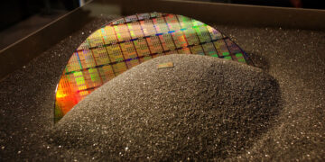
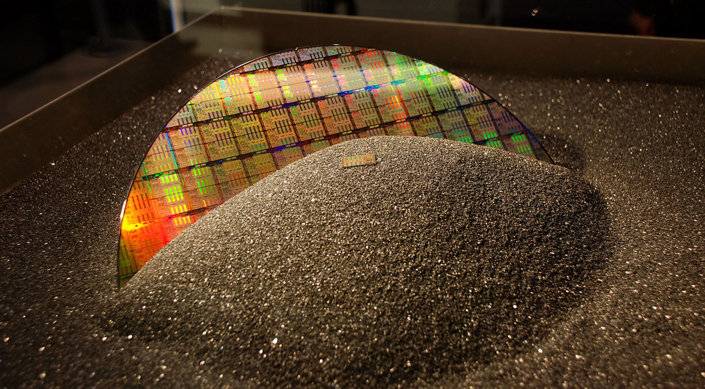
The Taiwan chip giant, TSMC, has revealed details about its next-gen processes. According to recent information, the A14 development is making impressive progress.
TSMC’s A14 Process Will Bring Massive Improvements Over N2 in Performance & Power-Efficiency
When examining the semiconductor firms discussing beyond 2nm, TSMC stands out. Intel Foundry has disclosed plans for their 14A process but hasn’t yet shared performance or yield figures. Now, based on information provided by TSMC (via Ray Wang), it is reported that TSMC’s A14 node has achieved “yield performance” ahead of schedule. More importantly, the Taiwan giant has revealed expected performance improvements over the N2 node; these are impressive.
TSMC’s A14 process is expected to be a significant release, contributing to Moore’s Law and the innovation of the computing segment in terms of performance. The more interesting point here is that despite the chip industry being ‘struggling’ with current-gen nodes like 3nm, TSMC is already discussing processes set for release years ahead. This strategy has maintained their dominance in the segment.
According to newer details, relative to the 2nm node, the A14 will bring a 15% higher speed at equivalent power consumption, resulting in up to 30% power-efficiency improvements. TSMC plans to use its second-generation GAAFET nanosheet transistors and new NanoFlex Pro standard cell architecture, which will increase density by up to 20% relative to N2. These improvements indicate that A14 will be pivotal for scaling performance.
Related Post


It will be interesting to see how significant a contribution the A14 makes to consumer products, given that companies like Apple, NVIDIA, and AMD are expected to adopt it. TSMC anticipates A14 entering production in 2028.


