


Login to Continue Learning
**SK Hynix Surpasses Both TSMC & Samsung with High-NA EUV System Integration, Setting New Standards**
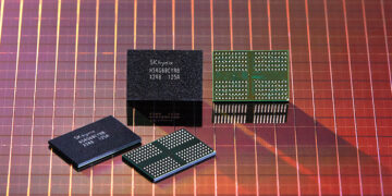
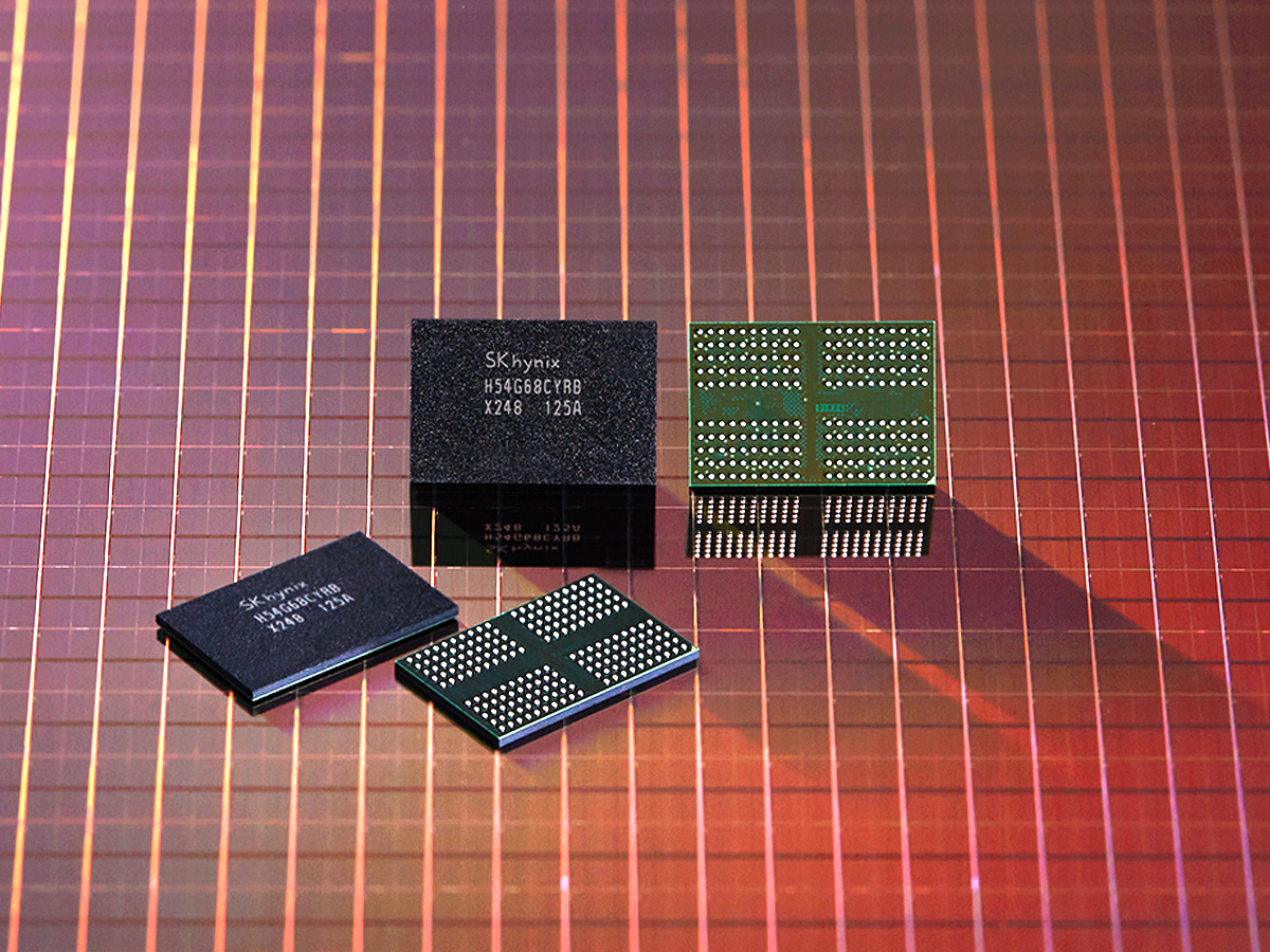
The Korean memory giant has become one of the largest and most advanced DRAM manufacturers thanks to its end-to-end solutions and partnership with NVIDIA. SK Hynix announced this achievement in a dedicated blog post, claiming that integrating ASML’s High-NA equipment will enable the development of cutting-edge products.
**Key Benefits of High-NA EUV Technology:**
– **Reduced Transistor Size:** The TWINSCAN EXE:5200B enables printing transistors 1.7 times smaller and achieving transistor densities 2.9 times higher than existing EUV systems.
– **Improved NA:** With a 40% improvement in the numerical aperture (NA), from 0.33 to 0.55, this new system significantly enhances precision.
Related Post


**Future Plans:**
With the adoption of the new system, SK Hynix plans to simplify the existing EUV process and accelerate the development of next-generation memory technologies. This will enhance product performance and cost competitiveness, while also strengthening its position in the high-value memory market.
**Previous Progress:**
In a past report, it was mentioned that SK Hynix would ramp up its DRAM technology to six EUV layers, marking significant progress. High-NA EUV equipment is essential for breaking the “layer benchmark,” and now that SK Hynix has access to ASML’s high-end machinery, it is evident that the company is poised for major advancements in the memory market.
**Industry Leadership:**
There’s no doubt that SK Hynix has positioned itself as the go-to spot for DRAM needs for clients like NVIDIA and AMD. The firm has also managed to dethrone industry leader Samsung in a relatively short time span. More importantly, integrating High-NA equipment is a testament to SK Hynix’s commitment to continuing to provide quality products and fierce competition.


