


Related Post


Login to Continue Learning
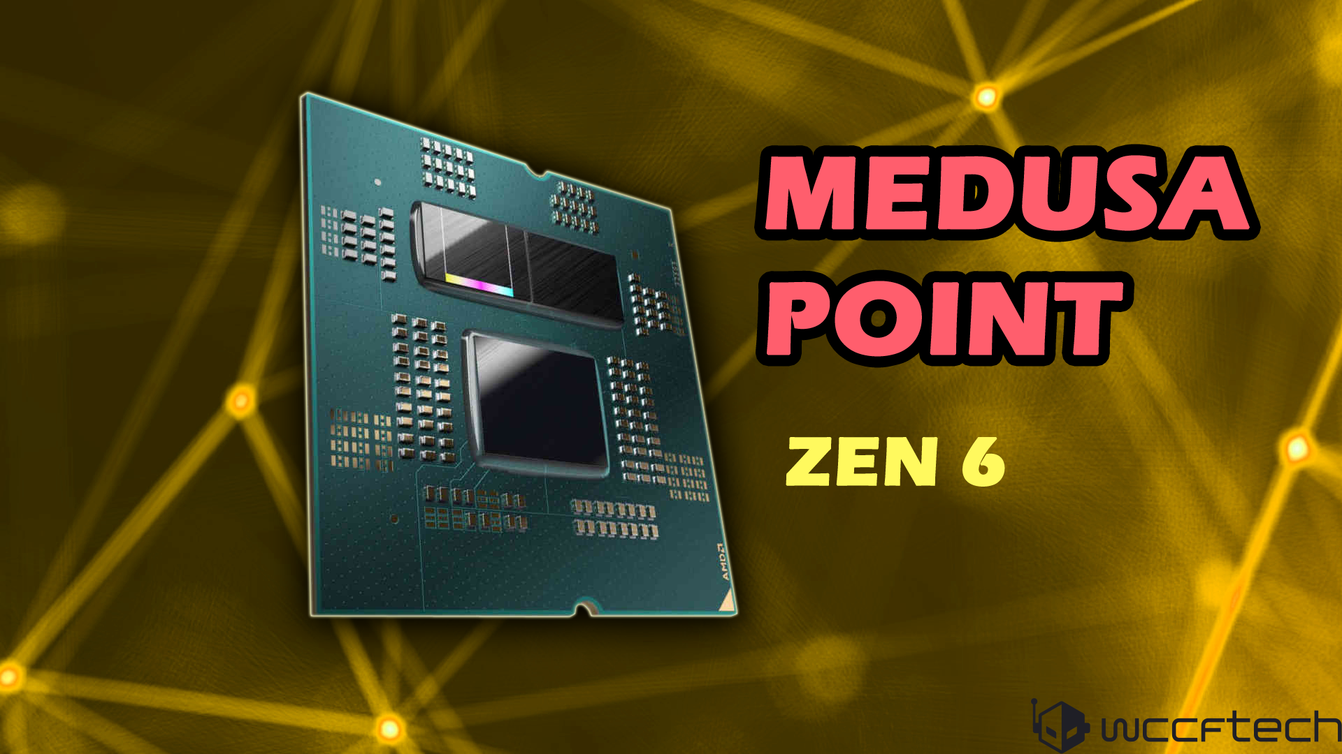
AMD has begun preparations for the next-generation processor lineup. In the latest NBD shipping manifest, it is clear that the Medusa Point will use the newer FP10 socket.
NBD Shipping Log Confirms Zen 6 Medusa Point Will Utilize a Bigger FP10 Socket and Be Rated at 45W
In March, Medusa Point was spotted in an NBD shipping log, indicating that it will use the newer FP10 socket, transitioning from the FP8 used by Strix Point. Another recent NBD shipping log confirms this and reveals that Medusa Point is likely being tested on AMD’s evaluation platform “PLUM.” This board supports a 45W TDP, which is a significant increase over the 28W of the Strix Point but can be boosted to up to 54W.

Medusa Point is based on the Zen 6 architecture and will power premium and mainstream laptops. It will be manufactured using TSMC’s 3nm process node and feature both Zen 6 and Zen 6c cores, similar to Strix Point. However, it is expected that Medua Point will have up to 22 cores, significantly more than its predecessor, but through a hybrid configuration including Zen 6, Zen 6c, and LP Zen 6 cores.

For integrated graphics, Medusa Point will retain the RDNA 3.5+ architecture, as RDNA 4 is exclusive to discrete GPUs. One can expect around 8 Compute Units, fewer than those in the Strix Point flagship chips but with a more refined architecture that offers better performance compared to traditional RDNA 3.5.
Medusa Point is expected to launch in late 2026, marking an early stage of development for Zen 6 processors.
News Source: @Olrak29_


