


Login to Continue Learning
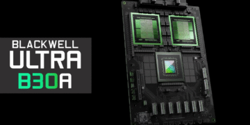
The NVIDIA Blackwell B30A GPU will use a single-chip design, unlike the dual-chiplets in standard Blackwell B200/B300 offerings. The Blackwell Ultra B300 solution, on the other hand, packs 50% more performance than the B200, 50% more memory, and twice the interconnect speeds. The top SKU will consist of two reticle-sized GPUs with a total of 15 PetaFLOPs FP4 compute and up to 288 GB HBM3e memory.
The new chip, tentatively known as the B30A, is expected to use a single-die design that delivers half the raw computing power of the dual-die configuration in Nvidia’s flagship B300 accelerator card. A single-die design refers to all main parts of an integrated circuit being made on one continuous piece of silicon rather than split across multiple dies.
The new chip will have high-bandwidth memory and Nvidia’s NVLink technology for fast data transmission between processors, similar to the H20, which is based on the company’s older Hopper architecture. Early reports suggest a significant demand for the B30A chip in China ahead of its launch.
If NVIDIA’s B30A is half the specification of the B300 chip, it can be expected to have up to 144 GB of HBM3e memory, an improvement over the H20’s 96 GB. However, the H20 also featured 41% fewer cores and 28% lower performance than the Hopper H100 configuration.
Related Post


NVIDIA hasn’t finalized the specifications but plans to deliver the first samples of the B30A Blackwell chip to a China-based client as early as next month. US President Donald Trump hinted at an unenhanced or castrated version of Blackwell for China, with Jensen possibly making a deal if there’s a 15-20% tariff on the said chips for China.
So it looks like the B30A will be the Blackwell chip given to China in the coming months. It will be interesting to see what specifications are finalized and how it compares to the true chip.


