


Login to Continue Learning
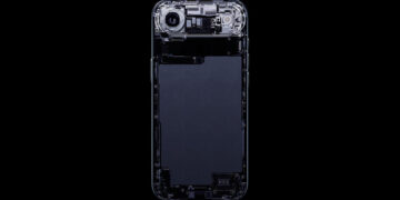
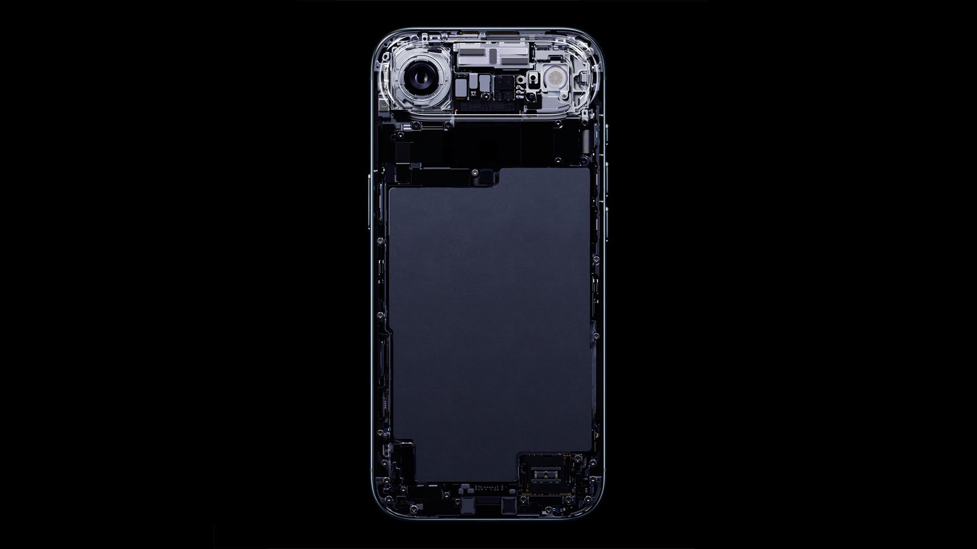
According to a motherboard design leak, only part of the A19 Pro chip is housed within the camera bump on the iPhone Air. The entire circuit board cannot fit due to space constraints; some areas need to be reserved for the battery and other components.
The iPhone Air’s motherboard is not entirely rectangular, making it impossible to place all its components solely in the camera bump. Instead, a significant portion of the logic board, including the A19 Pro, is located there. The rest of the PCB shares space with the battery. ShrimpApplePro shared schematics and labeling of the iPhone Air’s logic board, which show that the C1X 5G modem and N1 wireless networking chip are also present.
The design is a ‘sandwiched’ structure with components stacked on both sides to save space. @BasQuxFoo provided an illustration of how the iPhone Air’s logic board would look inside the device, clearly showing that only the A19 Pro is in the camera bump area.
Related Post


In a few generations, Apple might shrink future logic boards enough to fit them entirely in the camera cluster, with the remaining space occupied by a larger battery for extended runtimes. However, we should wait for official teardowns from reputable outlets to confirm this.


