


Login to Continue Learning
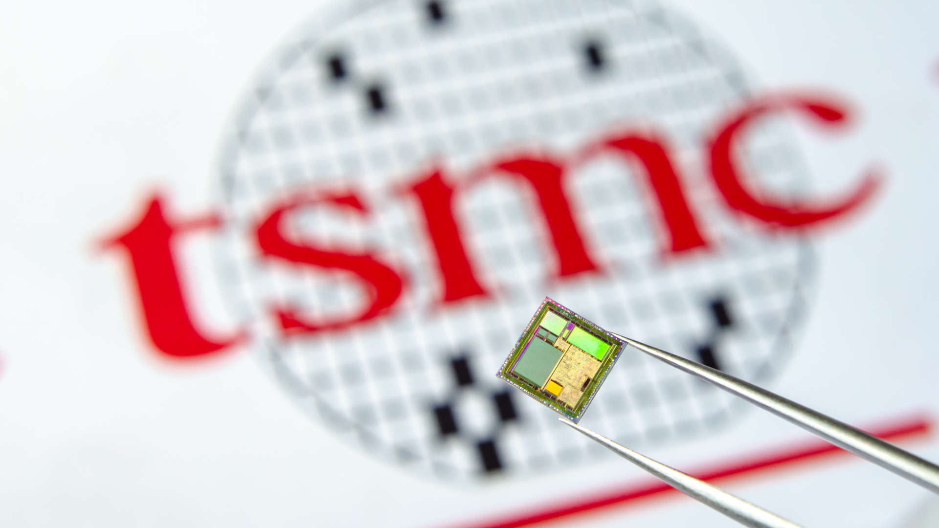
TSMC plans to start mass production of its 2nm process in the fourth quarter of 2025, as reported by WCCFtech. Although it will take several years for this technology to mature, TSMC is already rapidly advancing towards constructing a new facility that will manufacture 1.4nm wafers. The company is reportedly moving ahead of its original schedule and plans to break ground on a plant with an initial investment potentially reaching NT$1.5 trillion or approximately $49 billion.
The ‘Fab 25’ will house four production facilities, with TSMC racing to commence trial production on the 1.4nm technology by the end of 2027
According to a report from Economic News Daily, TSMC’s suppliers have already been informed about these plans in case they need to expedite equipment for 1.4nm production. The ‘Fab 25’ will be constructed at the Central Taiwan Science Park near Taichung City and will house four plants. The first plant is scheduled to undergo trial production by the end of 2027.
Based on this schedule, TSMC could start full-scale production by the second half of 2028, with a 15 percent improvement in performance and a 30 percent reduction in power consumption. The remaining three plants will also focus on 1.4nm wafer production. Although TSMC is aiming for an even more advanced lithography at 1nm, the report does not specify when trial production for this process will begin.
While it will take a couple of years before TSMC begins trial production, its 1.4nm process is expected to be costly. If the $30,000 per wafer cost for its 2nm node was already significant, imagine paying an estimated $45,000 per unit for the company’s A14 wafers.
Related Post


